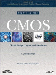
CMOS Circuit Design, Layout, and Simulation
The fourth edition of CMOS: Circuit Design, Layout, and Simulation is an updated guide to the practical design of both analog and digital integrated circuits. The author—a noted expert on the topic—offers a contemporary review of a wide range of analog/digital circuit blocks including: phase-locked-loops, delta-sigma sensing circuits, voltage/current references, op-amps, the design of data converters, and switching power supplies.
2019
A revised guide to the theory and implementation of CMOS analog and digital IC design
The fourth edition of CMOS: Circuit Design, Layout, and Simulation is an updated guide to the practical design of both analog and digital integrated circuits. The author—a noted expert on the topic—offers a contemporary review of a wide range of analog/digital circuit blocks including: phase-locked-loops, delta-sigma sensing circuits, voltage/current references, op-amps, the design of data converters, and switching power supplies.
CMOS includes discussions that detail the trade-offs and considerations when designing at the transistor-level. The companion website contains numerous examples for many computer-aided design (CAD) tools. Using the website enables readers to recreate, modify, or simulate the design examples presented throughout the book. In addition, the author includes hundreds of end-of-chapter problems to enhance understanding of the content presented. This newly revised edition:
• Provides in-depth coverage of both analog and digital transistor-level design techniques
• Discusses the design of phase- and delay-locked loops, mixed-signal circuits, data converters, and circuit noise
• Explores real-world process parameters, design rules, and layout examples
• Contains a new chapter on Power Electronics
Written for students in electrical and computer engineering and professionals in the field, the fourth edition of CMOS: Circuit Design, Layout, and Simulation is a practical guide to understanding analog and digital transistor-level design theory and techniques.
TABLE OF CONTENTS
1.1 The CMOS IC Design Process
1.2 CMOS Background
1.3 An Introduction to SPICE
2.1 Patterning
2.2 Laying Out the N-well
2.3 Resistance Calculation
2.4 The N-well/Substrate Diode
2.5 The RC Delay through the N-well
2.6 Twin Well Processes
Chapter 3 The Metal Layers
3.1 The Bonding Pad
3.2 Design and Layout Using the Metal Layers
3.3 Crosstalk and Ground Bounce
3.4 Layout Examples
Chapter 4 The Active and Poly Layers
4.1 Layout Using the Active and Poly Layers
4.2 Connecting Wires to Poly and Active
4.3 Electrostatic Discharge (ESD) Protection
5.1 Resistors
5.2 Capacitors
5.3 MOSFETs
5.4 Layout Examples
6.1 MOSFET Capacitance Overview/Review
6.2 The Threshold Voltage
6.3 IV Characteristics of MOSFETs
6.4 SPICE Modeling of the MOSFET
6.5 Short-Channel MOSFETs
7.1 CMOS Unit Processes
7.2 CMOS Process Integration
7.3 Backend Processes
7.4 Advanced CMOS Process Integration
7.5 Summary
8.1 Signals
8.2 Circuit Noise
8.3 Discussion
9.1 Long-Channel MOSFETs
9.2 Short-Channel MOSFETs
9.3 MOSFET Noise Modeling
10.1 The Digital MOSFET Model
10.2 The MOSFET Pass Gate
10.3 A Final Comment Concerning Measurements 341
R. Jacob Baker, CMOS Circuit Design, Layout, and Simulation, Jone Wiley & Sons 2019
 |  |  |
| CMOS Circuit Design, Layout, and Simulation | Electronic devices and circuit theory. Eleventh edition | The design of CMOS radio-frequency integrated circuits |
Thứ Ba, 18:53 21/02/2023
Copyright © 2018 Hanoi University of Industry.