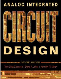
Analog Integrated Circuit Design
This edition features extensive new material on CMOS IC device modeling, processing and layout. Coverage has been added on several types of circuits that have increased in importance in the past decade, such as generalized integer-N phase locked loops and their phase noise analysis, voltage regulators, and 1.5b-per-stage pipelined A/D converters. Two new chapters have been added to make the book more accessible to beginners in the field: frequency response of analog ICs; and basic theory of feedback amplifiers.
2011
When first published in 1996, this text by David Johns and Kenneth Martin quickly became a leading textbook for the advanced course on Analog IC Design. This new edition has been thoroughly revised and updated by Tony Chan Carusone, a University of Toronto colleague of Drs. Johns and Martin. Dr. Chan Carusone is a specialist in analog and digital IC design in communications and signal processing.
This edition features extensive new material on CMOS IC device modeling, processing and layout. Coverage has been added on several types of circuits that have increased in importance in the past decade, such as generalized integer-N phase locked loops and their phase noise analysis, voltage regulators, and 1.5b-per-stage pipelined A/D converters. Two new chapters have been added to make the book more accessible to beginners in the field: frequency response of analog ICs; and basic theory of feedback amplifiers.
TABLE OF CONTENTS
CHAPTER 1 INTEGRATED-CIRCUIT DEVICES AND MODELLING
1.1 Semiconductors and pn Junctions
1.2 MOS Transistors
1.3 Device Model Summary
1.4 Advanced MOS Modelling
1.5 SPICE Modelling Parameters
1.6 Passive Devices
1.7 Appendix
1.8 Key Points
1.9 References
1.10 Problems
CHAPTER 2 PROCESSING AND LAYOUT
2.1 CMOS Processing
2.2 CMOS Layout and Design Rule
2.3 Variability and Mismatch
2.4 Analog Layout Considerations
2.5 Key Points
2.6 References
2.7 Problems
CHAPTER 3 BASIC CURRENT MIRRORS AND SINGLE-STAGE AMPLIFIERS
3.1 Simple CMOS Current Mirror
3.2 Common-Source Amplifier
3.3 Source-Follower or Common-Drain Amplifier
3.4 Common-Gate Amplifier
3.5 Source-Degenerated Current Mirrors
3.6 Cascode Current Mirrors
3.7 Cascode Gain Stage
3.8 MOS Differential Pair and Gain Stage
3.9 Key Points
3.10 References
3.11 Problems
CHAPTER 4 FREQUENCY RESPONSE OF ELECTRONIC CIRCUITS
4.1 Frequency Response of Linear Systems
4.2 Frequency Response of Elementary Transistor Circuit
4.3 Cascode Gain Stage
4.4 Source-Follower Amplifier
4.5 Differential Pair
4.6 Key Points
4.7 References
4.8 Problems
CHAPTER 5 FEEDBACK AMPLIFIERS
5.1 Ideal Model of Negative Feedback
5.2 Dynamic Response of Feedback Amplifiers
5.3 First- and Second-Order Feedback Systems
5.4 Common Feedback Amplifiers
5.5 Summary of Key Points
5.6 References
5.7 Problems
CHAPTER 6 BASIC OPAMP DESIGN AND COMPENSATION
6.1 Two-Stage CMOS Opamp
6.2 Opamp Compensation
6.3 Advanced Current Mirrors
6.4 Folded-Cascode Opamp
6.5 Current Mirror Opamp
6.6 Linear Settling Time Revisited
6.7 Fully Differential Opamps
6.7.1 Fully Differential Folded-Cascode Opamp
6.7.2 Alternative Fully Differential Opamps
6.7.3 Low Supply Voltage Opamps
6.8 Common-Mode Feedback Circuits
6.9 Summary of Key Points
6.10 References
6.11 Problems
CHAPTER 7 BIASING, REFERENCES, AND REGULATORS
7.1 Analog Integrated Circuit Biasing
7.2 Establishing Constant Transconductance
7.3 Establishing Constant Voltages and Currents
7.4 Voltage Regulation
7.5 Summary of Key Points
7.6 References
7.7 Problems
CHAPTER 8 BIPOLAR DEVICES AND CIRCUITS
8.1 Bipolar-Junction Transistors
8.2 Bipolar Device Model Summary
8.3 SPICE Modeling
8.4 Bipolar and BICMOS Processing
8.5 Bipolar Current Mirrors and Gain Stage
8.6 Appendix
8.7 Summary of Key Points
8.8 References
8.9 Problems
CHAPTER 9 NOISE AND LINEARITY ANALYSIS AND MODELLING
9.1 Time-Domain Analysis
9.2 Frequency-Domain Analysis
9.3 Noise Models for Circuit Elements
9.4 Noise Analysis Examples
9.5 Dynamic Range Performance
9.6 Key Points
9.7 References
9.8 Problems
CHAPTER 10 COMPARATORS
10.1 Comparator Specifications
10.2 Using an Opamp for a Comparator
10.3 Charge-Injection Error
10.4 Latched Comparators
10.5 Examples of CMOS and BiCMOS Comparators
10.6 Examples of Bipolar Comparators
10.7 Key Points
10.8 References
10.9 Problems
CHAPTER 11 SAMPLE-AND-HOLD AND TRANSLINEAR CIRCUITS
11.1 Performance of Sample-and-Hold Circuits
11.2 MOS Sample-and-Hold Basics
11.3 Examples of CMOS S/H Circuits
11.4 Bipolar and BiCMOS Sample-and-Holds
11.5 Translinear Gain Cell
11.6 Translinear Multiplier
11.7 Key Points
11.8 References
11.9 Problems
CHAPTER 12 CONTINUOUS-TIME FILTERS
12.1 Introduction to Continuous-Time Filter
12.2 Introduction to Gm-C Filters
12.3 Transconductors Using Fixed Resistors
12.4 CMOS Transconductors Using Triode Transistor
12.5 CMOS Transconductors Using Active Transistors
12.6 Bipolar Transconductors
12.7 BiCMOS Transconductor
12.8 Active RC and MOSFET-C Filters
12.9 Tuning Circuitry
12.10 Introduction to Complex Filters
12.11 Key Points
12.12 References
12.13 Problems
CHAPTER 13 DISCRETE-TIME SIGNALS
13.1 Overview of Some Signal Spectra
13.2 Laplace Transforms of Discrete-Time Signals
13.2.1 Spectra of Discrete-Time Signals
13.3 z-Transform
13.4 Downsampling and Upsampling
13.5 Discrete-Time Filters
13.6 Sample-and-Hold Response
13.7 Key Points
13.8 References
13.9 Problems
CHAPTER 14 SWITCHED-CAPACITOR CIRCUITS
14.1 Basic Building Blocks
14.2 Basic Operation and Analys
14.3 Noise in Switched-Capacitor Circuits
14.4 First-Order Filter
14.5 Biquad Filter
14.6 Charge Injection
14.7 Switched-Capacitor Gain Circuits
14.8 Correlated Double-Sampling Techniques
14.9 Other Switched-Capacitor Circuits
14.10 Key Points
14.11 References
14.12 Problems
CHAPTER 15 DATA CONVERTER FUNDAMENTALS
15.1 Ideal D/A Converter
15.2 Ideal A/D Converter
15.3 Quantization Noise
15.4 Signed Codes
15.5 Performance Limitations
15.6 Key Points
15.7 References
15.8 Problems
CHAPTER 16 NYQUIST-RATE D/A CONVERTERS
16.1 Decoder-Based Converters
16.2 Binary-Scaled Converters
16.3 Thermometer-Code Converters
16.4 Hybrid Converters
16.5 Key Points
16.6 References
16.7 Problems
CHAPTER 17 NYQUIST-RATE A/D CONVERTERS
17.1 Integrating Converters
17.2 Successive-Approximation Converters
17.3 Algorithmic (or Cyclic) A/D Converter
17.4 Pipelined A/D Converters
17.5 Flash Converters
17.6 Two-Step A/D Converters
17.7 Interpolating A/D Converters
17.8 Folding A/D Converters
17.9 Time-Interleaved A/D Converters
17.10 Key Points
17.11 References
17.12 Problems
CHAPTER 18 OVERSAMPLING CONVERTERS
18.1 Oversampling without Noise Shaping
18.2 Oversampling with Noise Shaping
18.3 System Architectures
18.4 Digital Decimation Filters
18.5 Higher-Order Modulators
18.6 Bandpass Oversampling Converters
18.7 Practical Considerations
18.8 Multi-Bit Oversampling Converters
18.9 Third-Order A/D Design Example
18.10 Key Points
18.11 References
18.12 Problems
CHAPTER 19 PHASE-LOCKED LOOPS
19.1 Basic Phase-Locked Loop Architecture
19.2 Linearized Small-Signal Analysis
19.3 Jitter and Phase Noise
19.4 Electronic Oscillators
19.5 Jitter and Phase Noise in PLLS
19.6 Key Points
19.7 References
19.8 Problems
Tony Chan Caruson, Analog Integrated Circuit Design, Jone Wiley & Sons, 2011
 |  |  |
| Design of Analog CMOS Integrated Circuits | Power system Scada and Smart Grids |
Thứ Ba, 17:27 21/02/2023
Copyright © 2018 Hanoi University of Industry.